Throw away the plug! Make wireless EV charging a reality now!
Unique components ensure safety, efficiency and reliability.
Think of an EV charging experience as seamless and intuitive as parking your car—just “park, charge, and go.” For the end user, the appeal is clear:
- No more heavy cables
- No fumbling with connectors
- No exposure to potentially dirty or damaged chargers
EV owners envision pulling into their garage, designated parking lot, or public charging station and easily charging their vehicle without leaving the driver's seat. This convenience makes everyday charging more convenient and improves safety by eliminating interfaces entirely.
Understanding this user-centric perspective is important for wireless EV charging system designers. By delivering efficient, reliable, and fast wireless charging, designers can unlock game-changing benefits that include convenience, comfort, and peace of mind for EV drivers.
While current wireless EV chargers can deliver up to 20 kW to charge batteries in four to six hours, future wireless chargers will deliver 100 kW and be able to increase the battery's state of charge by 50 percent in less than 20 minutes.1
Wireless charging stations must be fast, safe, efficient, and reliable to accelerate adoption.
This article explores the technological considerations and innovations needed to achieve this experience, ensuring wireless charging solutions meet the performance and user expectations in an ever-changing EV landscape. It presents four components that address the critical needs of creating designs that ensure charger circuit protection, safety monitoring, and fast, efficient power delivery.
Description of wireless charger
The wireless charger is an AC-AC converter that converts 50/60 Hz power to work in the 130 kHz frequency range. The resonant frequency depends on the topology and the Power semi conductor (Si/SiC/GaN) technology. Power delivery can reach 20 kW. Figure 1 shows a wireless charger and its load, EV. Main power and charge control circuit blocks and motor are also explained.

Safety and reliability considerations include overcurrent protection, overvoltage protection, overtemperature protection, and low current monitoring. Improving efficiency requires designing with low power loss components. Figure 2 shows the components that provide circuit protection and high efficiency circuits in a typical wireless charger design. Sensors provide temperature monitoring and enclosure access protection.
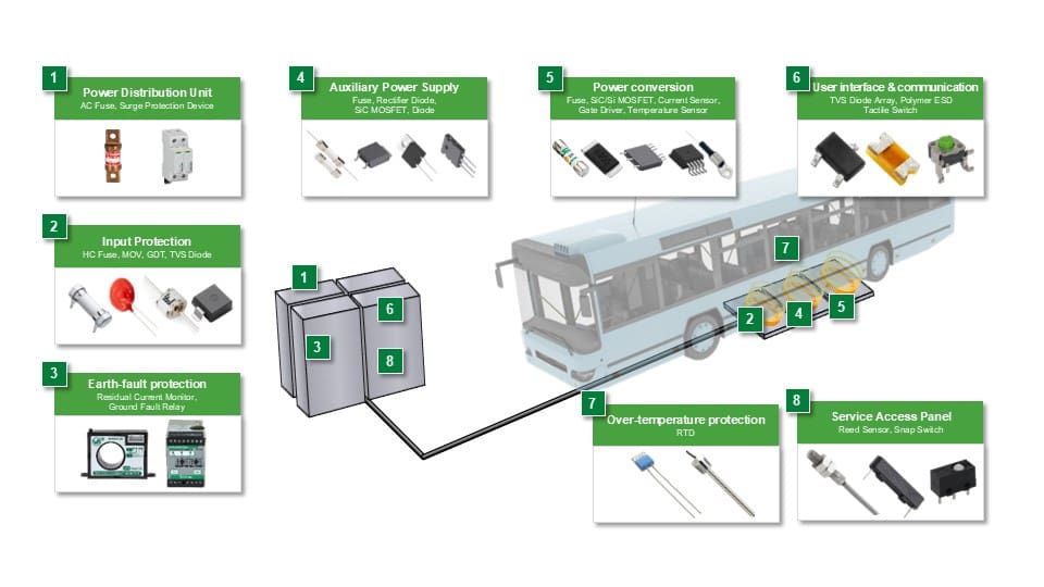
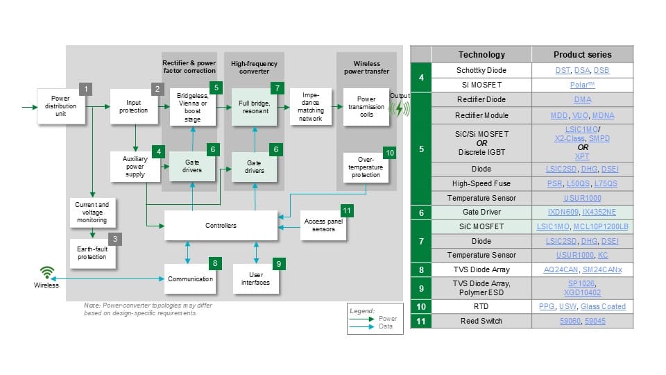
Figures 3 and 4 show an example of a wireless charger in a more detailed block diagram. The adjacent table in Figure 3 lists the components that equip the charger with protection against electrical hazards. Figure 4 mainly shows the components that produce good performance and sensitive hearing.

Circuit protection and security components
The Input Protection Circuit houses the main overcurrent and over temperature protection components. Recommended components include a high current fuse for the power supply circuit and a fast acting fuse to protect the auxiliary power supply and control circuit. A metal oxide varistor (MOV) in series with the discharge tube absorbs overvoltage transients. Overvoltage changes are caused by lightning that can induce voltage surges in AC input lines. In addition, switching the load on and off can cause the AC line voltage to rise.
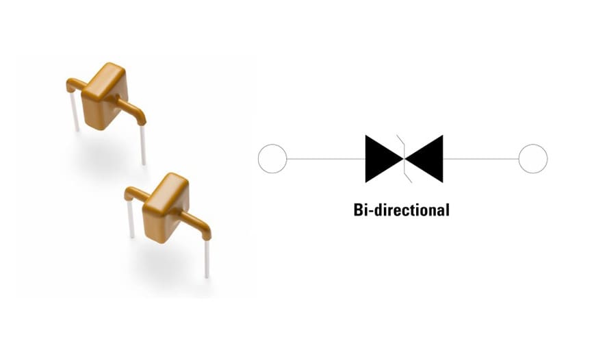
A special component that can capture the transient voltage components that have passed through the MOV and discharge tube is the transient voltage suppressor (TVS) diode. TVS diodes have lower clamping voltages, and operate much faster than MOV devices. Special diodes can ensure the protection of the downstream circuit. They can absorb a pulse of one kA and respond in less than one nanosecond. TVS diodes can provide protection against electrostatic discharge (ESD) in air up to 15 kV and direct discharge up to 8 kV. Bi-directional models and models less than one-tenth the size of traditional differential solutions are available. A TVS diode can have an axial lead or a surface mount form factor. Figure 5 shows a TVS diode and its functional diagram, using i AK1-Y Series TVS Diode from Littelfuse for example. This component will provide the necessary protection from both ESD and other transients to avoid damage to the semiconductor circuitry in the wireless charger.
With systems such as wireless EV chargers, low voltage monitoring is essential to protect workers. Earth Fault Protection Circuit performs low current monitoring function. Littelfuse offers new residual current monitors for this circuit that detect both AC and DC ground fault currents. New series, i RCMP20 Residual Current Monitor Series for Mode 2 again Mode 3 wireless charging stations, provides a large open current transformer to support high AC charging currents. The remaining current monitors have sensitive trip limits, 4.5 mA DC and 22 mA AC. In addition, monitors use integrated conductors with high cross-sectional areas to provide better heat management and reduce the temperature rise of the printed circuit board (PCB). The result is a compact and reliable design that does not sacrifice performance. In addition, the monitors have high immunity to electromagnetic interference (EMI), which improves the reliability of the charger circuit and reduces false circuit trips. Monitors can be mounted horizontally or vertically to allow designers the flexibility to make the most of the space. Figure 6 shows models in the Residual Current Monitor series. (Watch the video.)

Components to increase efficiency and reliability
Systems, such as wireless charging systems, use a large amount of energy. Optimizing the design for efficiency reduces energy consumption and utility costs and reduces heat build-up. The reduced heat generated lowers the internal temperature of the system and improves system reliability. The use of two components in the power delivery circuit can contribute to higher efficiency and greater reliability. The two components are gate drivers and SiC MOSFETs.
Gate drivers control Power SiC MOSFETs and IGBTs in a Bridgeless, Vienna, or Boost Rectifier and Full Bridge, Resonant High-Frequency Converter circuit. The drivers have 9 A discrete source and sink outputs, allowing programmable on and off timing while minimizing switching losses. An internal negative charge regulator provides selectable negative gate bias for improved dV/dt protection and fast turn-off. Gate drivers reduce switching times with on and off propagation delay times of typically 70 and 65 nanoseconds. A typical value for the rise time and fall time is ten nanoseconds.
To ensure robust performance, the gate drivers have a sunset detection circuit that senses the overstate of the SiC MOSFET and initiates a soft turn-off. This circuit prevents a potentially dangerous dV/dt event. Additional protection features include UVLO detection and thermal shutdown. Figure 7 showsLittelfuse IX4352NE SiC MOSFET and IGBT Driver IChigh-speed gate driver with features that provide reliable SiC MOSFET control.

High power SiC MOSFETs drive the power transmission coils. Half-bridge packages have a Drain-Source voltage of 1200 V and a drain current of up to 19.5 A. As well as delivering high power, MOSFETs reduce power consumption in the state with a typical RDS(ON) minimum 160 mΩ. SiC MOSFETs have low switching power loss due to common gate charging, short turn-on, delay times, and current rise and fall times.
The DCB-based insulated package improves heat resistance and power handling capability. An improved topside cooling package makes thermal management easier. I Littelfuse half-bridge SiC MOSFET MCL10P1200LB Seriesshown in Figure 8, produces higher efficiency with improved packaging to reduce the number of parts and improve higher reliability.

Contact an expert for a reliable wireless charging solution
Protection against electrical hazards such as overcurrent, overvoltage, ESD, and overheating is essential to ensure reliable operation. The four recommended components described in the previous sections enable designers to develop robust, safe, and reliable EV charging stations.
In order to develop a robust and efficient product, designers should consider using application engineers from the manufacturer's components to save design time and compatibility costs. Application developers can help with the following:
- A selection of cost-effective protection, sensors, and high-performance components
- Knowledge of applicable security standards
- Littelfuse can perform pre-compliance testing to avoid compliance testing failures and save on project delays and additional costs of multiple compliance testing cycles.
Working with the manufacturer's application engineers and using recommended components will help produce robust, reliable and efficient wireless EV charging solutions.
To learn more about circuit protection, sensors, and power management solutions for wireless EV charging design, download the guide, Best Charging Solutions for EV Charging Stations, The rating of the company Littelfuse, Inc.
Contact Littelfuse for more information on making your wireless charging design safe, efficient and reliable.

References:
1L. Blain. World's fastest wireless EV charger unlocks 100 kW parking spaces. The new Atlas. March 18, 2024.